


|
|
|
|
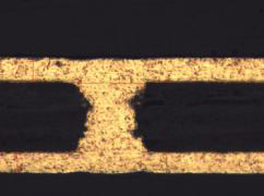
孔径(Blind hole diameter):60um 介质厚度(Dielectric thickness):68um 电镀厚度(Copper surface thickness):17um 电流密度(Current density):2.5ASD |
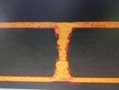
孔径(Blind hole diameter):86um 介质厚度(Dielectric thickness):210um 电镀厚度(Copper surface thickness):20um 电流密度(Current density):2.5ASD |
1.薄面铜(17-22um镀铜厚度即可完成相关通孔填孔)
Copper etching is unnecessary due to thin copper surface plated(17 to 22um).
2大电流密度可缩短电镀时间,并提高生产效率
High current density will shorten plating time and improve productivity.
3. 副产物低,药水稳定性高,定期进行活性碳处理即可维持长期性能稳定
Low by-product, highly stable bath and long-time stable performance realized by regular activated carbon treatment.
4. 适用于闪镀和无需闪镀流程。
Applicable to flash and no flash process.
5.各添加剂均可CVS分析
Additive agents can be analyzed by CVS.