


SBF-530 series
|
|
|
|
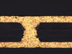
Blind hole diameter:60um Dielectric thickness:68um Copper surface thickness:17um Current density:2.5ASD |
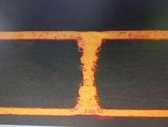
Blind hole diameter:86um Dielectric thickness:210um Copper surface thickness:20um Current density:2.5ASD |
1.Copper etching is unnecessary due to thin copper surface plated(17 to 22um).
2.High current density will shorten plating time and improve productivity.
3.Low by-product, highly stable bath and long-time stable performance realized by regular activated carbon treatment.
4.Applicable to flash and no flash process.
5.Additive agents can be analyzed by CVS.